At this rate they'll be manufacturing 0nm chips soon, and in a decade they'll be on -1nm.
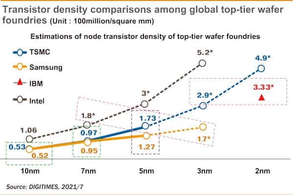
But despite the weird naming scheme, it's clear from transistor density [1] and GPU prices [2] that foundries are still making progress in transistors per dollar. That progress is just barely beginning to make large neural networks (Stable Diffusion, vision and speech systems, language model AIs) deployable in consumer applications.
It might not matter whether your cell phone renders this page in 1ms or 10ms, but the difference between talking to a 20B parameter language model and a 200B net is night and day [3]. If TSMC/Samsung/Intel can squeeze out just one or two more nodes, then by the middle of the century we might have limited general-purpose AI in every home and office.
As a traditional "web dev" kind of hacker, I feel like I'm just sitting idly by while a massive transition happens underneath me.
I understand roughly why this shift is happening (machine language proving to solve a whole raft of hard problems) and how it's happening (specialized chip designs for matrix math). But I don't understand where it's all going, or how I can plug into it.
It feels like a fundamentally different landscape than what I'm used to. There's more alchemy, perhaps. Or maybe it's that the truly important models are trained using tools and data that are out of reach for individuals.
Does anyone else feel this way? Better yet, has anyone felt this way and overcome it by getting up to speed in the ML world?
As a web developer, you are primed to create the interfaces to these ML tools (or any tool really). The browser is the most widespread UI application that nearly every single consumer computer has access to. You can work on literally anything that someone accesses via the internet, and the more AI/ML is made useful, the more people will need access to these products, the more web devs will be needed to build apps to use these products
Not only for building user-facing tools; the AI/ML space needs a lot of good engineering practices to function. In many cases, traditional software, infra and DevOps, QA and UI engineers, etc., are as crucial to ML projects as data scientists are.
So I don't think you need to worry about being left behind or that your skills are stagnating if you're not directly developing ML models. There's no existential reason to jump in, unless you're particularly interested in ML.
> So I don't think you need to worry about being left behind or that your skills are stagnating if you're not directly developing ML models.
Aren't ML models kind of the front lines these days? If I'm understanding correctly, it's the models, the training techniques, the curation of data sets-- These are the things that will inform the next generation of products and services.
I agree that there's more to it that just letting ML models loose, but it certainly seems like the core of it.
Depends on what you want to focus on. My point is that there are plenty of roles adjacent to the core of ML that are still needed to make ML function. Think about data storage for models, maintaining CI pipelines for training, UIs for curation and labeling, packaging and deploying models, data version control systems, etc. None of these are tasks data scientists should be concerned about, and viceversa, data science is not something engineers should necessarily be concerned about either. It doesn't make either role superior; they just complement each other well.
This makes me hopeful for the future of my career, but as a n00b in regards to CS principles, it still kinda sucks that the minutia of this technology is so foreign to me. I think that is what the OP was getting at.
Using ML/AI tools is not terribly difficult, and the principle of how they work is simple enough (feed the model examples of what you want, eventually it can reproduce similar ideas when prompted or recognize new examples as something that it's seen before). Maybe it's ignorance on my part in regards to what it takes to learn these technologies deeply, but right now, I wouldn't even know where to begin to start studying to really learn how this technology works/operates on a fundamental level.
Despite my ignorance of the subject, I could probably work out how to step into an ancient archaic COBOL system or whatever, but ML/AI _feels_ so far out of my reach as a webdev.
This is one reason I think ML as a topic is cool, even if I think the practical uses for the every day person is still really far away from being a realistic.
As a wise dog once said, "sucking at something is the first step towards being kinda good at something."
I avoided many areas of computer science and programming for far too long because I thought they were "hard". Many of them turned out to be way easier than I expected (I often found myself wondering, "why didn't someone tell me how easy this is! I could have done this years ago!!"), or so much fun that working on them felt effortless, despite the increased effort in objective terms.
I guess what I'm saying is, start learning about what interests you today! Make small and consistent progress.
I've found that setting aside time every day (rather than just when I feel like it) to study areas of interest has been extremely helpful in this regard.
It's not something that's out of reach for a web dev. It might seem like an insurmountable task, but if you break it down, you can digest it easier.
ML is just math. We're at a point where you don't even have to completely grok the math to apply ML techniques productively.
If you want somewhere to start and need a project idea, read up on how to build a simple binary classifier. The "hard" work is building good training and validation sets if you use a ML framework.
The practical deep learning course from fast.ai is what I've been working my way through, at a much slower pace, I am sure, than someone would if they were writing code for a living. The difficult technical hurdles are getting used to (i) Python if you've never used it and (ii) Jupyter notebooks if you've never used them. I'm using Paperspace.com for my GPU instances.
Thanks for the link! I'll put it on the list of other stuff to check out. I don't write Python at work, but it's probably something I should familiarize myself with a little more since it's pretty popular in the Home Automation communities.
Just like every other technological advance, there is a sort of "food chain" that builds on top of these foundational technologies. You didn't have to work in cryptography to play a role in the massive proliferation of online commerce and banking. There were and are many, many conventional tasks and non-PhD-making innovations between cryptography existing and the wonderful low-friction commerce we now enjoy.
Don't know how language translation models work? No problem, use one that someone else made to make a web framework that self-internationalizes to the user's browser default language without the site creator even knowing that language exists!
That's certainly true! I can use my current skillset to help connect users with new tech. And there have been many minor revolutions during the course of my career, many of which have been incorporated into the sort of work I do.
I guess the difference (for me, anyway) is that this change isn't incremental. It's a fundamentally new type of computing-- One that comes with a totally new way of approaching problems. Listening to Andrej Karpathy talk about Software 2.0, for instance, it seems probable that ML has a place in many parts of the stack.
It's possible I'm just projecting my insecurities, here, but my experience has been that changes to computing hardware usually result in changes across the entire industry. And this feels like a pretty meaningful change.
The ML space is a lot easier to get into than before. Training and using models is more and more just like using any other library or framework. The hard algorithmic parts, the math, that's all being solved by academia and researcher.
That said, getting hold of the data and the computational resources for training are barriers.
I'll be bold enough to make the contrarian prediction. The approach of throwing ever more parameters in the model and ever more transistors on the chip is at best a brute force approach to AI and will likely plateau in effectiveness long before we get to "general purpose AI". We do not need 1nm neurons running at GHZ rates and training on a corpus of everything ever said just to comprehend language. There needs to be an algorithmic breakthrough. There is likely already more than enough processing power.
Even bolder prediction: When we finally understand how the brain actually does it, the algorithmic improvement will be so enormous that the machine learning tasks which run on massive servers today will be able to run on the phone currently in your pocket.
This view may ultimately be right, but massively ignores the current observed trends in capabilities increase[0], scaling laws[1], and things like grokking[2]. I'm seeing an increasing amount of researchers (me included) moving to stances like: "there is a scary possibility that we may solve all the benchmarks we come up for AI... without understanding anything fundamentally deep about what intelligence is about.
a bummer for those like me who are see AI as a fantastic way to unlock deeper insights on human intelligence" @Thom_Wolf [3]
I feel the same way. What if there’s a better way to use those transistors?
The semiconductor researchers spend a lot of effort to make ever-smaller transistors. What is a transistor? It’s a tiny switch.
The ML researchers meanwhile use the language of linear algebra to define mathematical transformations of real numbers with nice differentiability properties.
The chipmakers are then tasked with reconciling the two. So they use transistors to make gates. And gates to make adders. And adders to make integer multipliers. And integer multipliers to make floating point multipliers. And fp multipliers to implement matrix multiplication. And now you can run your cat diffuser model on those transistors.
But what is the chance that the configuration of transistors in a floating point multiplier is anywhere close to the most efficient transistor configuration for learning?
The only reason we’re using multiplication of real numbers is because the math people said so.
Since we are openly speculating, I think the missing ingredient is feedback loops. There is no explicit input side and output side of the brain. Its all just a ball of neurons. There is propagation delay between the neurons. This makes it possible to have self sustaining loops of neurons firing. The longer the loop, the longer the amount of time it takes to go full circle. We call this phenomena "brain waves".
I think what we get wrong is that individual neurons rarely represent anything. They are a medium for the waves. The waves are the currency of thought. A brain is a series of electro-mechanical oscillators that resonates with abstract concepts and patterns.
AFAIK, most research is still using the old "neurons represent single things" paradigm. Someone needs to tell them, there's no such thing as a "grandmother neuron".
> When we finally understand how the brain actually does it
If you dig into how neurons work in the brain you'll discover that a single neuron has the complexity of a large neural network internally and it's behavior is not nearly as simple as the typical model explanation. Different ion channels, time-dependent behavior, up/down regulation of neurotransmitter receptors and release, and much more.
It is entirely possible that the brain "does it" by throwing vastly more computing resources at the problem than we previously believed.
I have and while its true a neuron does more than the simple on/off of their artificial peers, I'd hardly call it "the complexity of a large neural network internally". There just aren't that many bits needed to represent all the parameters you just mentioned. Stuff you mention like ion channels and neurotransmitters feels like excessively mimicking biological constraints rather than something actually relevant. Who cares if the real neurons use chemical channels and electrical channels to communicate, the artificial ones can just send the same information in electrical channels for everything.
While brain has vastly more computing resources, they are probably operating very far from the theoretical optimum. There must be so much baggage, inefficiency and dead pathways left which do not have much purpose at all. The brain was evolved, not designed, which means that any random features/mutations which did not inhibit individuals ability to procreate got to stay.
I think that even when we understand the brain completely, it will be very difficult disentangling what is useful for artificial neural networks and what doesn't really matter.
The capabilities are already there. If the compute becomes more affordable, they will explode in usage. In fact, this is already happening. See live transcription on newer iOS devices for an example.
Scaling diagrams also showed no sign of plateauing AFAIK.
>At this rate they'll be manufacturing 0nm chips soon, and in a decade they'll be on -1nm.
The industry has chosen angstroms as the next unit. Where 1.4nm will becomes 14A. ( Intel for now, but TSMC has uses the term in a few of its presentation )
>If TSMC/Samsung/Intel can squeeze out just one or two more nodes,
We have a very solid roadmap all the way to 1nm, or 10A by the end of this decade. As long as the market is willing to pay for it. At least TSMC 3nm and 2nm is pretty much done.
>limited general-purpose AI in every home
Like the comment below, I am not convinced the brute force approach works. You can already build a 800mm2 NPU today that is equivalent to a chip used in "in every home and office." by the end of this decade. But we are still no where near it.
>"That progress is just barely beginning to make large neural networks (Stable Diffusion, vision and speech systems, language model AIs) deployable in consumer applications."
Interesting. Is Stable Diffusion a product of neural network size then? Is the size of the network a function of chips density?
Also is there a Stable Diffusion app that currently works on edge devices?
so this is again one of these "material x was slightly better in a lab experiment" -> "we conclude that it certainly can be used as part of a complex technology" press releases.
I am not too fond of this, but obviously thats the easiest way to explain the significance of research results.
Getting a new material into a semiconductor manufacturing process takes years or even decades. Whatever material will be in TSMCs "1nm" process, it is already known.
I remember 15 years ago reading about EUV litography and a lot of people were saying that it looks like a pipe dream because they don't know of any way to produce a EUV light source strong enough, outside nuclear explosions and the like.
It took 25 years to commercialize EUV. And that is from the point where a decision was made to industrialize it, not from the first scientific report about EUV radiation.
It looks like small piece of tin is where the magic begins [1]:
> An EUV system uses a high-energy laser that fires on a microscopic droplet of molten tin and turns it into plasma, emitting EUV light, which then is focused into a beam.
is the spectrum naturally pure, or is there some filtering/selection going on?
> The tricky thing with EUV light is that it’s absorbed by everything, even air. That’s why an EUV system has a large high-vacuum chamber in which the light can travel far enough to land on the wafer. The light is guided by a series of ultra-reflective mirrors
ahahah, that's not even the craziest thing about EUV. it's that the whole process has two actual laser shots, there is a preshot that heats the tin, forms a plasma that is shaped like a lens. and then comes the stronger, main shot.
So it took about 10 years to get into production. OP isn't claiming it's impossible, just that it's far from being practical. You could definitely say that about EUV 15y ago
Yes, but do you remember all the BS PR releases about new "promising" techniques and materials that would "revolutionize" this or that process, that we read 15 and 20 and 30 years ago, that never materialized at all?
The rumor I heard was that HP licensed all the rights to the tech away and development has stalled since no entity can put their hands on enough of the IP to do anything with. : / So development has pretty much stalled since the last time HP showed of The Machine with memristors.
Patents on fractal compression and related techniques are all expired now. There might still be people who remember how to use them. Do we see any use of it, now?
IMO compression was a lot more important when we had modems and disk sizes measured in megabytes or single digit gigabytes. Once you have "good enough" compression then you solve most issues and in many areas where there used to be compression they've been increasingly removing it. Compression causes latency after all and some of the biggest impediments to processing speed now is latency.
So unlike before, compression has stopped being a primary driving factor in the engineering of many types of devices and types of software.
Raw data compression was once an attractive application, but the method is more general. That said, streaming services still pay a great deal for bandwidth and storage in edge nodes. Cell- and keyframe-oriented video compression are reaching their limit.
We are still interested in feature extraction and scene composition, which both benefit from more compact representation.
To compete with hardware-assisted decoding in display hardware, fractal rendering would probably need to be coded to run in Vulkan.
I take the slightly more patient approach with this. LCD used very old discoveries, something need to mature through a few industrial cycles before it gets discarded I guess.
World is full of technologies that would be cool if you also had a Time Machine. But other tech outpaces is so if it is born behind it never takes off.
Some of it is pretty fun for playing what if with (enforced) pastoralism. Using primitive materials with a modern understanding of them, instead of limiting yourself to historically accurate processes.
It's funny that it's debatable what's a memristor and what's not: "Intel has stated that 3D XPoint does not use a phase-change or memristor technology, although this is disputed by independent reviewers." (Wikipedia)
Reading the article I wondered if tapered interconnects were the solution. Fat interconnects with thin fins? Probably harder to calculate inductance and capacitance, but these people deal with complexity all day.
Not entirely sure how you’d avoid voids with tapers facing upward, but you can orient them in five out of six directions. And I’ve seen a few examples of the weird games they have to play with light to get the crisp corners they are after so maybe tapers would be easier?
The actual discovery is reported in one of the last paragraphs:
>The breakthrough relates to a new set of materials that can create monolayer—or two-dimensional (2D)—transistors in a chip to scale the overall density by a factor matching the number of layers. The teams at TSMC and MIT have demonstrated low resistance ohmic contacts with a variety of existing semiconductor materials, including molybdenum disulfide (MoS2), tungsten disulfide (WS2), and tungsten diselenide (WSe2).
So it is a better way to make a contact to a semiconductor material that noone knows how to manufacture reliably on a large area wafer.
Could we finally, get a diagram, you know a 100dpi PNG, with a 3D representation of the most constraint logic transistor at 3/2/1nm with all the metric quotes?
> Using non-silicon materials facilitates very tiny transistors—as small as 1 nm. However, as TSMC researchers acknowledge, the 1-nm process node is not likely to be used for years to come.
Several kinds of semiconductor materials are used for high power or high frequency applications but only at much larger process nodes. For example Gallium Nitride, InP, SiGe.
Gallium could only produce microchips larger than silicon. What we need are diamond microchips which should outperform silicon chips by a factor of 23K and be a third smaller.
It seems we're still a long ways off from diamond semiconductors becoming mainstream. I wonder what the forcing function will end up being to dethrone silicon.
Germanium is bigger, right? It’s used in DSP chips and now in power transformers. The fact that it’s used for high frequency circuitry has always made me wonder why we don’t do large scale chips in it. Surely cheaper than the acrobatics we are doing for <5nm, no?
It’s used in current-dense applications and leakage current is out boogeyman with silicon.
I have some background in this space in undergrad. Non Si materials are used in industry, germanium is used in some special applications and i believe its the #2 semiconducting material, however it is harder to use than Si because it's very difficult to keep it clean of impurities. Not the doping kind.
The first transistors were made of germanium, and before germanium diodes were made from selenium and from an oxide of copper. Crystal radios commonly used Schottky diodes made of galena. Gallium arsenide is big business.
This is great and all, but in the end it just buys us a few more years. Something more radical has to come along eventually if we want to continue a Moore-esque pattern.
I wonder what happened to plans for optical interconnects?
I’m going to love seeing all these gains eaten alive by adware and js and general modern software bloat, while the common user does the same functions on the computer they've been doing since the 1990s (email/web browsing/document writing).
Getting so tired of this knee jerk complaint. Do you design standard cell libraries or analog ASIC IPs? If not, why would you care that "1nm" doesn't correspond to an actual dimension in the process? I work with ASIC design in a node where the name still matches the minimum gate length, and the number of times this has actual mattered to me is exactly zero.
What does matter to most people is transistor density and other performance metrics that actually have an impact on the product. The "Xnm" has always given a rough indication of the improvements in transistor density, and all the foundries has done is continue to name the nodes as if that's what matters... which is indeed the case.
TSMC does sometimes call the nodes eg "N7" now. But nobody that matter cares because everyone understands that "7nm" is a marketing term.
Why doesn't the industry want to create a new metric?
Like 2 bil transistors/square cm, let's call it 2 btsc or something. Surely they use something like that internally, why not publicly? Maybe there are different kinds of "transistors", some (CPU) bigger than others (RAM)?
I work in chip design on single digit "nm" processes.
Interally we might say 5nm to refer generally and N5 or N5P to refer to a specific process. When you need more specific numbers you look it up. Exact design parameters are carefully protected trade secrets.
Commenters on Hacker News care a lot more about this distinction than the engineers working with it. Nobody cares that it is not gate length or half pitch.
The number of transistors per square centimeter will vary a lot depending on application. High speed logic is less dense than power efficient logic is less than RAM, for example. I suppose you could use a metric like a minimum size 8T SRAM cell but then you'd have complaints about foundries gaming the system by making process choices to shrink that at the expense of other structures.
Intel kind of tried this. In their presentations when they were struggling with 10nm, they tried focusing on transistor density count. That failed; people remained confused, especially with the (nm)+++ convention for same-node improvements. Intel gave up their old naming convention last year and are now using a marketing naming scheme similar to TSMC/Samsung.
Moreover, density is only one metric of improvement, the other major one is power efficiency. Foundries want to market these improvements too.
A mass misbelief in the continuation of Moore's law into impossible sub-molecular scales. There is no more low-hanging fruit of "just make the optics more precise to make the lithograph smaller"; every process-node step we're taking now is rather a "side-step" involving solving increasingly-complex puzzles to make the same-sized features do more per molecule. It's code golf, at a hardware level. And as in code golf, there's a pretty low ceiling as to how intricately interwoven features can become. You can't eliminate the fundamental need to have all those features in the code (circuit) in some sense.
The actual visible effect of this is an economic one: we've gone from spending linearly more marginal CapEx per fab process-node upgrade, to spending geometrically more marginal CapEx. Each process node under 8nm has been twice as costly to design as the one before it. This is untenable.
The particular measurements of the elements are not interesting, but the transistor densities are meaningful. I would expect a 1nm chip to achieve densities 100x a 10nm chip. That seems unlikely.
It's not a deception, the transistor itself is 1nm, the gate is larger because of physics. We're talking transistor and gates composed of 100~ freaking atoms with transistors being in the dozen or so. And we are complaining that they're using the "wrong metrics." We are nearing Moores limit, might as well rejoice when they bleed out another nm or so and can pack in a few billion more transistors.
The active part of a FET is the area that is under the gate or surrounded by the gate.
It makes no sense to speak about a transistor that would be smaller than the gate, there is no such thing.
Besides the active part, whose conductance is controlled and variable, the transistor includes parts that are either electrical conductors, like the source , the drain and the gate electrode, or electrical insulators.
While those parts may be less important than the active part, they also have a major influence on the transistor characteristics, by introducing various resistances and capacitances in the equivalent schematic.
What matters is always the complete transistor. The only dimensions in a current transistor that are around 1 nm are vertical dimensions, in the direction perpendicular on the semiconductor, e.g. the thickness of the gate insulator.
The 2D semiconductors that are proposed for the TSMC "1 nm" process are substances that have a structure made of 2D sheets of atoms, like graphite, but which are semiconductors, unlike graphite, which is a 2D electrical conductor.
In this case the thickness of the semiconductor can be reduced to single layer of atoms, which is not possible with semiconductors that are 3D crystals, like silicon, because when they no longer form a complete crystal their electrical properties change a lot and they can become conductors or insulators, instead of remaining semiconductors.
There is little doubt that for reducing the transistor dimensions more than it is possible with a 3D semiconductor like silicon, at some point a transition to 2D semiconductors will be necessary. It remains to be seen when that will be possible at an acceptable cost and whether such smaller transistors can improve the overall performance of a device, because making smaller transistors makes sense only when that allows a smaller price, smaller volume or higher performance of a complete product.
> So many people believe that it is the actual gate size
They never state it was the actual gate size in the first place. May be you should blame the media for it?
And just to reply to parents.
> TSMC does sometimes call the nodes eg "N7" now.
It is not sometimes. TSMC has always been very careful and calling it N7 or N10 all the way back to 28nm era. What the media, marketing and other PR decided to call it are entirely different matter. This is especially problematic since ~2015 when they have gotten thousands if not millions times more media coverage.
Language drifts. You might as well be upset that a British pound is longer a pound of silver. Or that people now use "very", "really", and "literally" as intensifiers rather than as claims to absolute truth.
Investors. Even more sophisticated investors can be bamboozled by various claims. Because investors are usually trying to pick the future winners, they need these things as proxies to determine who is actually going to have the faster chips, or the lower costs, etc.
Analysts are often not from the exact line of business. They may have a bachelor's in engineering, or something, but they're usually not domain experts beyond having studied the field from a business perspective and gotten used to its lingo. So, these things can be kind of manipulative. That said, it's par for the course. It's better than outright lying and bribing the analysts like in the 2000-2002 telecom bust.
Colloquially lots of successful technologies have been referred to as "AI" and so it doesn't seem that unreasonable that investors could look into that kind of stuff. On the other hand, if somebody's investing strategy assumes, like, artificial general intelligence is coming soon -- investing involves risk and investing while stupid involves disproportionate risk I guess.
> Since when is it acceptable to trick laypeople, especially when laypeople are buying products with the false advertising (cpus...)?
This is such a HN issue. It's not tricking people because the vast majority of layman don't even care about node size, gate size or the manufacturing process. The number of times I have encountered a person outside of a tech bubble that cared about the manufacturing process of a CPU is exactly zero.
What people do care about: does it work, is it fast, is it efficient and can I afford it. At least for performance and efficiency the marketing term does give a somewhat reliable indication of the generational gains.
Depends on the instruction mix I guess, right? I'm sure you could come up with different benchmarks (think of the silly case, brancy hard-to-predict code on one of those super-long-pipeline Pentiums).
Processors are just fundamentally complicated and boiling them down to a couple number is hard. Any modern one is pretty good and saying anything more than that -- depends on your workload I guess.
Wait -- based on the graphic at that page, should we be taking away that TSMC's and Samsung's shipping 6nm chips have only a very slight transistors/mm^2 advantage over Intel's 10nm chips? And just as importantly, that "XXnm" is nothing more than a marketing tool?!
Hyperbole aside, it's undeniable that TSMC's chips for Apple have a greater computing-power/watt than Intel's chips -- but is that all they bring to the table? I don't mean to disparage power efficiency, it's awesome. But the question stands.
This comment is there under every article that has nm in it. For the millionth time, 1 nm should be read as "1 nm equivalent". The purpose of the naming is to continue to scale with density.
But despite the weird naming scheme, it's clear from transistor density [1] and GPU prices [2] that foundries are still making progress in transistors per dollar. That progress is just barely beginning to make large neural networks (Stable Diffusion, vision and speech systems, language model AIs) deployable in consumer applications.
It might not matter whether your cell phone renders this page in 1ms or 10ms, but the difference between talking to a 20B parameter language model and a 200B net is night and day [3]. If TSMC/Samsung/Intel can squeeze out just one or two more nodes, then by the middle of the century we might have limited general-purpose AI in every home and office.
[1] https://en.wikipedia.org/wiki/Transistor_count#GPUs
[2] https://pcpartpicker.com/trends/price/video-card/
[3] https://textsynth.com/playground.html